Analyzing Semiconductor Failure
Perry L. Martin
What follows is a brief description of how to properly perform semiconductor failure analysis without introducing unwanted artifacts into the analysis.
Semiconductor devices are almost always part of a larger, more complex piece of electronic equipment. These devices operate in concert with other circuit elements and are subject to system, subsystem and environmental influences. When equipment fails in the field or on the shop floor, technicians usually begin their evaluations with the unit’s smallest, most easily replaceable module or subsystem. The subsystem is then sent to a lab, where technicians troubleshoot the problem to an individual component, which is then removed–often with less-than-controlled thermal, mechanical and electrical stresses–and submitted to a laboratory for analysis. Although this isn’t the optimal failure analysis path, it is generally what actually happens.
Isolating the Subsystem or Component Responsible for the Semiconductor Failure
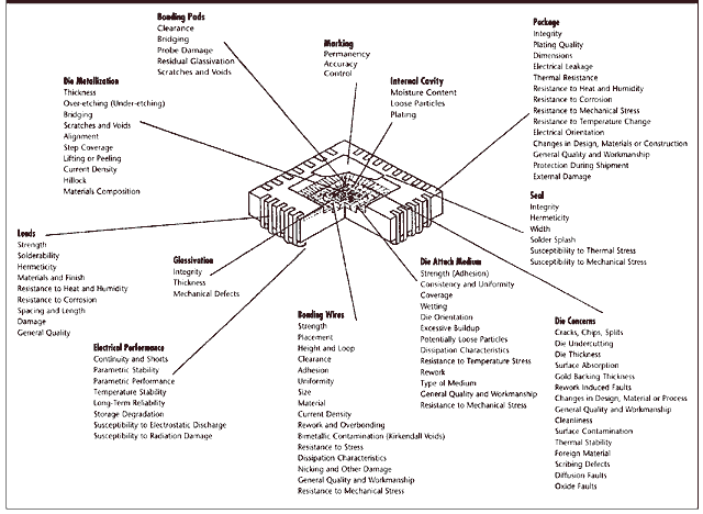
Once laboratory technicians identify the subsystem responsible for the semiconductor failure, the failed section is then further isolated to the board or smallest mechanical structural level containing all faulty parts and components. Figure 1 identifies some of the primary device reliability concerns.
The ultimate goal in failure analysis is to arrive at an accurate determination of the cause of the semiconductor failure. In semiconductor failure analysis, destructive testing is usually necessary in a large portion of the analytical effort. Decapsulation, scribing metal and cross sectioning are all acceptable techniques, but when they’re performed prematurely, these procedures can result in irreversible damage and a ruined analysis. Thus, the analyst must consider the potential damage and purpose of each task and remember the rule followed by carpenters: “Measure twice and cut once.”
Electrical Component Failure Verification
Electrical test verification is an essential step in characterizing the suspect device and establishing its role in the circuit malfunction. Electrical testing is also performed to compare the device’s present condition with specified parameters and operation at different temperature extremes. However, electrical testing or verification may not be possible if the device is badly damaged. At other times, failure validation may not be possible because the device performs within its electrical specifications when it’s tested. If validation is impossible, the analyst must determine the appropriate method for testing or examining the failed device.
Care must be observed in the removal of electronic components to avoid introducing secondary damage, as when technicians who are only interested in getting the equipment back in service clip leads and pry packages off circuit boards. If the device cannot be patched up to perform an electrical check, optical examination may be the only alternative.
Noted anomalies must be analyzed with cause and effect in mind. An electrical overstress site on a cracked die in a broken integrated circuit package might have occurred prior to lid removal and could be the cause of the semiconductor failure. It’s essential that repair personnel be educated about the importance of ESD precautions and general component handling and care.
Low-Power Stereo Zoom Optical Microscopy
Failure modes readily identified by the low-power stereo microscope include contaminants on the package surface (often located between the leads), which can cause electrical leakage or shorts; fractured or broken dielectrics or glass seals; fractures in weld seams, blow holes, voids, etc; broken leads or loose feed-through pins; and arc-over or burns across the dielectrics.
Medium-to high-power Optical Microscopy
The medium- to high-power optical microscope, generally used to accentuate a failure mode already detected by other means, is especially effective for examining fractures in leads, plating and glass-to-metal seals; chemical damage to nonconductive glasses; and small defects in weld zones.
Particle Impact Noise Detection (PIND)
PIND test systems are used to detect loose particles within a device that has an unfilled internal cavity. The analyst would typically perform a PIND test on a device whenever the suspected failure mode indicated high leakage, intermittents or a short. An open circuit would not usually be caused by loose particles but may be detected if the open circuit is caused by a loose bondwire. However, if the part fails the PIND test, it must be decapped to verify the nature of the particle causing the semiconductor failure because the PIND test cannot differentiate between conductive and nonconductive particles.
X-ray Radiography
X-ray radiography is a good method for nondestructive analysis of most device types. The analyst should inspect for encapsulated foreign material, internal open circuits and shorts, and changes in alignment due to the encapsulation process. When properly performed, X-ray analysis will not alter or affect either the device or its failure mode.
This Technique Offers Two Major Benefits for the Failure Analyst:
- A graphic representation of internal or covered characteristics of the device or sample under inspection prior to any cutting, depotting or handling.
- A graphic representation of how the device is constructed. This enables the analyst to formulate effective disassembly procedures.
Scanning Acoustic Microscopy
Scanning acoustic microscopy (SAM) uses the absorption and reflection of ultrasonic waves in a sample. This technique is especially sensitive to any change in acoustic impedance such as debonds or delamination (as can occur in a plastic encapsulated device). These types of faults are very difficult to resolve using X-ray techniques. Typical applications for SAM include the evaluation of die-attach integrity, detection of voids in the molding compound, characterization of wire bonds and identification of cracks in the die or molding compound.
Hermeticity Testing
Hermeticity testing is used to determine the integrity of the device’s encapsulation. The purpose of encapsulation is to seal gases or fluids inside the device’s package and to prevent gases or fluids from leaking in. The thin-film nichrome resistor provides a good example of what can happen from moisture intrusion; high moisture and gases attack these devices on internal surfaces that have no protective plating, resulting in corrosion and failure. Moisture also attacks semiconductor devices by physical corrosion, electrical leakage and shorts.
To determine the package integrity of these devices and other components, failure analysts may use a gross leak tester or a fine (helium tracer gas) leak tester. Gross leak, or bubble leak testers, utilize fluorocarbon liquids for indications. Fine leak testing is performed using digital helium mass spectrometers. The device being analyzed is pressurized in helium gas, then tested for outgassing helium in the detector. However, a leak test may not always be required. Hermeticity testing is a secondary failure analysis tool generally used to aid the analyst in postulating the probable cause of failure.
Residual Gas Analysis (RGA)
Knowledge of the gas type inside a package can be crucial. Many electrical components are hermetically sealed in dry nitrogen. If a salt moisture atmosphere is found inside, corrosion and electrical leakage failures are quite possible.
Water vapor content and residual gas analysis (RGA) are performed using the same basic technique. Outgassing of lubricants, which then condense on relay contacts, can increase contact resistance on the relays at low currents and voltages. Outgassing of epoxies in hybrid circuits, which subsequently condense on die surfaces, can lead to electrical leakage failures. Depending upon the materials and systems involved, RGA should only be performed by those certified in the technique. Even then, inaccuracies and inconsistencies can be a problem.
Vacuum Bake
Low-temperature vacuum drying of a package can be performed to dry out suspected external moisture or evaporate volatile contaminants without exposing internal components to elevated temperatures. Recovery of the device after a low-temperature vacuum drying would strongly suggest that moisture had been absorbed or trapped on the external surfaces. A low-temperature bake with a hole punctured in the package removes moisture and volatile gases from the package interior. Recovery after this procedure would suggest that trapped internal moisture or volatile contaminants had been present.
When the semiconductor failure is caused by ionic contamination or slow state/bound charge leakage path, such as inversion layers, a bake at high temperature can “heal” or reverse degraded electrical characteristics by dispersing the charges on the die. This indicates that the device failed due to a manufacturing fault rather than electrical damage from external means. Electrical parts that have been irreversibly damaged by external overstress conditions do not heal by a simple bake.
External Cleaning
External washing during device failure analysis may be advisable. Deionized or distilled water washes, acetic acid washes, solvent washes and plasma cleaning are typically used wash types. Solvent washes are recommended when minimal effects on metals and glasses are desired. The use of ultrasonics can cause damage. Fluorine-based plasma cleaning is recommended for glasses, and oxygen-based plasma cleaning is used for organics.
Package Opening, Decapsulation
The goal of decapsulation is to expose the semiconductor failure and internal construction of the device without altering the failure mode. The appropriate technique for device opening is generally mechanical or chemical.
Mechanical techniques usually apply to metal, glass and ceramic packages and typically require jeweler’s tools, whereas chemical techniques are generally used on plastic- or epoxy-encapsulated devices. For example, chemicals are the logical choice for removing die coatings. Acid etching involves the use of hot sulfuric acid, fuming nitric acid, hydrofluoric acid, phosphoric acid or hydrochloric acid. Most acids, however, are generally not very selective; they will attack materials indiscriminately. Commercial depotting chemicals are available for more selective decapsulation.
Internal Visual Examination
Following decapsulation, internal examination can be achieved by the use of optical microscopes or the scanning electron microscope (SEM). SEMs have the additional ability to perform voltage contrast and electron-beam-induced current analysis of devices under biased conditions. Biased devices can also be examined with high-magnification infrared thermography, which can identify hot spots that command interest as possible failure sites. An ultraviolet microscope can be used for the evaluation of organic contamination.
Surface Analysis
An energy-dispersive X-ray analysis (EDXA) attachment to the SEM is a valuable tool in failure analysis because it can use the generated X-rays of the SEM to analyze the material composition. When the sample under observation is bombarded by a high-energy beam of electrons, X-rays are given off that impinge on the silicon surface of the EDXA detector. The penetration depth of the X-rays into the silicon is a direct function of the energy of the X-ray. Along the penetration track, interaction occurs between the X-ray and silicon atoms, creating hole-electron pairs. The currents generated are sampled and the magnitude of pulses related to signal output is usually a multichannel spectral output with peaks at specific energies, representing X-rays for the various elements present in the specimen being observed in the SEM. The major advantage of the EDXA system is the detection of the entire energy/elemental spectrum simultaneously.
More highly specialized contaminate surface analysis techniques include auger electron spectroscopy (AES), energy spectroscopy chemical analysis (ESCA), secondary ion mass spectroscopy (SIMS), wavelength dispersive X-ray (WDX) analysis and electron microprobe (EMP) analysis. Determination of oxides and nitrides are a significant advantage of the EMP over EDXA. AES may involve ion etching of the surface, resulting in a depth profile on the contaminant being analyzed. ESCA utilizes valence state information of the material present on the surface of the device and provides excellent resolution of the various carbon compounds. ESCA is an excellent analytical tool for determining the molecular structure of polymer coatings and the identification of chemical states. SIMS is the most sensitive of all techniques and is the only instrument capable of directly measuring dopant profiles in a semiconductor.
Microsectioning
During the course of failure analysis, it’s sometimes appropriate or necessary to cross-section the sample. The goal of cross sectioning or microsectioning is to expose internal features of components and their packaging.
Size, complexity and target usually differentiate the cross sectioning of semiconductor devices from the more typical metallurgical samples. Many of the physical features and subcomponents are quite small, while the complexity lies in the wide variety of materials that can be encountered in a single specimen. A specified target could be a shorted junction area with a feature size of 1 micron. The experience required to hit such targets is largely acquired through practice.
Analyzing the Evidence and Determining the Failure Mode
After the analyst has accumulated enough evidence to formulate preliminary conclusions, subsequent investigation should be directed toward confirming the probable cause and eliminating other possibilities. As new facts modify first impressions, different hypotheses of the semiconductor failure will develop, which the analyst can retain or abandon as the findings dictate. During the analysis, it’s important to recognize work that doesn’t produce useful results. Negative evidence may be helpful in dismissing some causes of failure from consideration.
Perry L. Martin developed the Electronic Failure Analysis Laboratory in Sacramento, California, for National Technical Systems. He has taught at Loyola University and California State University, Sacramento, and frequently teaches in-plant failure analysis seminars through Technology Seminars Inc. Martin is the author of Electronic Failure Analysis Handbook (McGraw-Hill, 1999). Contact him by e-mail at pmartin@qualitydigest.com.
Related Articles

Martin Sprocket and Gears: Maintenance and Troubleshooting Guide

Reliability Tips: The Layers of Root Cause

An Integrated Process for System Maintenance, Fault Diagnosis and Support

Implement a Cost Effective Root Cause Problem Elimination (RCPE) Process

Hydraulic Cylinder Failure Caused by the Diesel Effect

RCFA of Bearing Failure